Table of Contents
- The Reticle Limit and the Yield Problem
- Why Yield Falls With Die Size
- What a Chiplet Design Looks Like
- Mixing Process Nodes Deliberately
- The Interconnect Is the Hard Part
- Advanced Packaging Approaches
- What Chiplets Cost
- Where This Is Heading
- Common Misconceptions
- Conclusion
- Frequently Asked Questions
Key takeaway: Large monolithic dies fail economically because defect probability scales with area. Chiplets keep individual dies small, which keeps yield high, and let designers use expensive advanced nodes only for the parts that benefit from them.
The Reticle Limit and the Yield Problem
Two physical constraints ended the practice of simply building bigger chips.
The first is the reticle limit. Photolithography projects a pattern through a mask onto the wafer, and the mask has a maximum field size — roughly 26 by 33 millimetres, giving a maximum die area around 858 square millimetres. A design larger than that cannot be printed in one exposure. Techniques exist to stitch exposures together and they are expensive and constrained.
The second is yield, and it is the more consequential of the two. Manufacturing defects occur at a certain density across a wafer, distributed roughly randomly. A larger die covers more area, so it is more likely to contain a defect, so a larger fraction of large dies are unusable.
These constraints arrived alongside a third change: advanced process nodes stopped delivering the cost-per-transistor reduction that made shrinking automatically economical. Newer nodes are faster and more power-efficient, and the cost per wafer has risen enough that cost per transistor is roughly flat or increasing.
Together these mean the historical strategy — shrink the process, build a bigger monolithic die, ship more performance for the same price — no longer works. Chiplets are the industry’s structural response.
Why Yield Falls With Die Size
The relationship is worth understanding numerically because it explains the entire economic argument.
Consider a wafer with a defect density of 0.1 defects per square centimetre. For a die of area A, the probability of containing no defects declines exponentially with area.
| Die area | Approximate yield | Good dies per 300mm wafer |
|---|---|---|
| 50 mm² | ~95% | ~1,180 |
| 100 mm² | ~90% | ~560 |
| 400 mm² | ~67% | ~100 |
| 800 mm² | ~45% | ~33 |
The numbers are illustrative and the shape is what matters. Doubling die area more than doubles the loss rate, because each additional square millimetre is another opportunity for a defect.
Now compare two ways of building the equivalent of an 800 mm² processor. As one monolithic die, roughly 45 percent of attempts are usable. As eight 100 mm² chiplets assembled together, each chiplet yields around 90 percent — and defective chiplets are discarded individually rather than taking the whole processor with them.
The saving is substantial and it compounds with wafer cost. On an advanced node where a wafer costs a great deal, discarding a 100 mm² piece instead of an 800 mm² piece is the difference between a viable product and an unviable one.
This is the core argument, and everything else about chiplets is a consequence of it.
What a Chiplet Design Looks Like
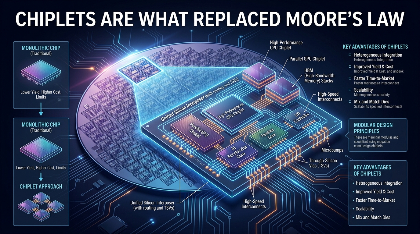
Rather than one die containing everything, a processor becomes several dies in one package.
A common partitioning:
Compute dies. The processor cores. Small, replicated, manufactured on the most advanced node available because cores benefit most from density and efficiency.
Input-output dies. Memory controllers, high-speed serial links, and external interfaces. These are dominated by analogue circuitry that scales poorly with process shrinks, so they are built on a mature, cheaper node.
Cache dies. Sometimes separated and stacked vertically, since dense memory has different optimal process characteristics than logic.
Accelerator dies. Specialised units — media encoding, machine learning inference, cryptography — included or omitted per product variant.
The flexibility this creates is a significant secondary benefit. One compute chiplet design serves an entire product range: four of them for a mid-range part, sixteen for a high-end one, combined with different input-output dies for different market segments. Instead of designing and validating a separate monolithic die per product tier, you design a small number of chiplets and combine them.
That reduces design cost, which at advanced nodes has become enormous — mask sets and verification for a leading-edge design run into very large sums. Amortising one chiplet design across many products changes that calculation.
Mixing Process Nodes Deliberately
The insight that makes chiplets more than a yield workaround: different circuit types have genuinely different optimal manufacturing processes.
Logic benefits substantially from advanced nodes. Smaller transistors switch faster and consume less energy, so cores get meaningfully better.
Analogue and mixed-signal circuits benefit little. Their performance depends on device matching and voltage headroom, which advanced nodes do not improve and sometimes worsen.
Input-output circuitry must drive external signals at specific voltages, which constrains how small the transistors can usefully be.
Dense memory has its own optimal process characteristics, different from logic.
In a monolithic design, everything is manufactured on whichever node was chosen, which means paying advanced-node prices for analogue and input-output circuitry that gains nothing from it. In a chiplet design, each function uses the node that suits it.
The economic effect is large, because advanced-node wafer costs are considerably higher than mature-node costs. Moving the input-output and analogue portion — frequently a substantial fraction of total die area — to a mature node while keeping cores on the leading edge reduces cost without reducing performance.
This is why chiplet adoption accelerated even for designs that would fit within the reticle limit. The yield argument justified it initially; the node-mixing argument makes it advantageous regardless.
The Interconnect Is the Hard Part
Splitting a chip creates a communication problem where none existed. On a monolithic die, two blocks communicate over on-chip wiring at very low latency and energy cost. Across chiplets, signals must cross a package boundary.
The properties that determine whether a chiplet design performs well:
Bandwidth. Modern processors move enormous quantities of data between cores and memory. The interconnect must not become the bottleneck.
Latency. Every additional nanosecond of inter-chiplet latency affects performance, particularly for cache-coherent traffic where cores must maintain a consistent view of memory.
Energy per bit. Moving data costs energy, and moving it across a package costs considerably more than moving it on-die. In power-constrained designs, interconnect energy can become a significant fraction of the total.
Coherency. Cores on different chiplets sharing memory must maintain cache coherence across the package boundary. This is the genuinely difficult engineering problem, and it constrains how far chiplets can be separated.
The energy point deserves emphasis because it is a real cost rather than a solved problem. Inter-chiplet communication is fundamentally more expensive in energy terms than on-die communication, which means chiplet designs accept a power penalty in exchange for the yield and cost benefits. Advanced packaging reduces the penalty; it does not eliminate it.
Standardisation efforts are addressing the interface layer, with the goal of chiplets from different vendors interoperating in one package. That would create a market for chiplets as components rather than as internal design choices, which is a substantial potential shift and remains largely prospective.
Advanced Packaging Approaches
How chiplets are physically connected determines the achievable bandwidth and latency.
Organic substrate. Chiplets on a conventional package substrate, connected by traces. Cheapest, lowest bandwidth density, longest connections. Adequate where inter-chiplet traffic is modest.
Silicon interposer. Chiplets mounted on a piece of silicon containing the wiring. Silicon supports far finer wiring than organic substrates, giving much higher connection density. More expensive, and it is what high-bandwidth memory integration generally requires.
Silicon bridges. Small silicon pieces embedded in an organic substrate, providing dense connections only where needed. A cost compromise between the two above.
Direct vertical bonding. Chiplets bonded face to face with connections between them, no intervening substrate. Shortest possible connections, highest density, lowest energy per bit. The most advanced and most expensive option, and it introduces thermal challenges because stacked dies are harder to cool.
Full 3D stacking. Several layers with vertical connections through the silicon. Highest density and the most severe thermal constraints, since heat from lower layers must pass through upper ones.
Thermal management is the constraint that limits vertical stacking. Heat generated in a lower die must escape through the dies above it, and silicon is a mediocre thermal conductor in that direction. This is why stacking is currently applied selectively — memory on logic, where the memory layer generates relatively little heat — rather than stacking high-power logic on high-power logic.
What Chiplets Cost
The trade-offs are real and worth stating plainly.
Packaging complexity and cost. Advanced packaging is a sophisticated manufacturing step with its own yield considerations. A design can lose good chiplets to packaging failures.
Known-good-die testing. Chiplets must be tested before assembly, because assembling a defective chiplet wastes the good ones alongside it. Testing an unpackaged die is harder than testing a packaged one.
Interconnect energy. A permanent power penalty relative to monolithic integration.
Latency penalty. Inter-chiplet communication is slower than on-die communication, which affects workloads sensitive to memory latency.
Design complexity. Partitioning a design across chiplets, defining the interfaces, and verifying the assembled system is more complex than designing one die.
Thermal density. Concentrating compute chiplets creates hot spots that a spread-out monolithic die would not have.
The consequence is that chiplets are not universally advantageous. For small dies where yield is already high, monolithic integration remains simpler, cheaper, and better performing. Chiplets win where the equivalent monolithic die would be large, where node mixing saves meaningfully, or where product-range flexibility justifies the packaging cost.
Where This Is Heading
Several developments are worth watching.
Interface standardisation aiming at chiplets from different vendors interoperating. If this matures, chip design becomes more like board design — selecting components rather than designing everything.
Optical interconnect for inter-chiplet communication, which would substantially change the energy and distance constraints. Currently at the research and early-product stage.
Backside power delivery, routing power through the wafer’s reverse side to free the front for signal routing. This is a manufacturing change with implications for how densely chiplets can be connected.
Increased vertical stacking as thermal solutions improve, since vertical connections are shorter and more efficient than lateral ones.
Specialised chiplets as products. Rather than every vendor designing their own accelerator, purchasing a chiplet that does it.
The direction is consistent: away from the monolithic die as the unit of chip design, toward the package as the system. Which is a genuine architectural shift rather than an incremental one, and it is why the industry describes chiplets as the successor to straightforward process scaling rather than as a manufacturing detail.
Common Misconceptions
“Chiplets are just multi-chip modules.” Multi-chip modules placed complete, independent chips in a package. Chiplets are partial designs that only function assembled, with interconnect designed as part of the architecture.
“Chiplets are always cheaper.” Only where the monolithic equivalent would be large or where node mixing saves meaningfully. Small dies are cheaper monolithic.
“Chiplets make Moore’s Law continue.” They address the economics of scaling, not the physics. Transistors are not getting smaller faster because of chiplets.
“More chiplets is better.” Each boundary costs latency and energy. Partitioning is an optimisation with a cost, not a free improvement.
“Chiplets solve the thermal problem.” They frequently worsen it, by concentrating compute and by enabling stacking that traps heat.
Conclusion
The historical approach to chip improvement — shrink the process, build a bigger die — stopped working for two reasons. Defect probability scales with die area, so large dies yield poorly, and advanced nodes stopped reducing cost per transistor.
Chiplets address both. Keeping individual dies small keeps yield high, and discarding a defective 100 mm² piece is far cheaper than discarding an 800 mm² one. Separating functions by their optimal process node means paying advanced-node prices only for the logic that benefits, while input-output and analogue circuitry uses mature, cheaper manufacturing.
The costs are genuine: advanced packaging is expensive and has its own yield, inter-chiplet communication carries a permanent energy and latency penalty, and concentrating compute creates thermal challenges that stacking makes worse.
Which is why chiplets are not universally correct. They win for large designs, for node mixing, and for serving a product range from a small number of validated components — and monolithic integration remains better for small dies where yield was never the problem.
Frequently Asked Questions
Why does yield fall so sharply with die size? Defects are distributed roughly randomly across a wafer, so a larger die is more likely to contain one. The relationship is exponential in area rather than linear, which is why doubling die size more than doubles the loss rate.
Is a chiplet processor slower than a monolithic equivalent? For latency-sensitive workloads, somewhat — crossing a package boundary costs more than on-die communication. The performance loss is usually smaller than the cost saving justifies, and advanced packaging narrows it.
Why not manufacture everything on the newest node? Analogue and input-output circuitry gains little from advanced nodes while costing far more per unit area. Mixing nodes means paying the premium only where it buys performance.
What limits vertical stacking? Heat. Lower layers must dissipate through upper ones, and silicon conducts heat poorly in that direction. This is why stacking is applied selectively rather than generally.
Are chiplets from different vendors interchangeable? Not yet in practice. Standardisation efforts aim at this and adoption is early. Currently chiplets are generally designed together as a system.
Do chiplets extend Moore’s Law? They address the economics rather than the physics. Transistor scaling continues to slow; chiplets make it economically viable to build large, capable processors despite that.
Is advanced packaging a bottleneck? Capacity for the most advanced packaging types has been constrained, and it is a specialised manufacturing capability with a limited number of suppliers. That concentration is a genuine supply consideration for the industry.