

Table of Contents
- The Wavelength Wall
- Why 13.5 Nanometres Is So Difficult
- Generating the Light
- Mirrors Instead of Lenses
- The Mask Problem
- Multipatterning and Why EUV Was Worth It
- High-NA and the Next Step
- A Supply Chain With One Path
- Common Misconceptions
- Conclusion
- Frequently Asked Questions
Key takeaway: Every leading-edge chip is patterned by machines from a single supplier, using light produced by vaporising tin with a laser, reflected off mirrors polished to atomic flatness, in a vacuum. There is no second source and no near-term alternative.
The Wavelength Wall
Photolithography prints circuit patterns by projecting light through a mask onto a light-sensitive coating on a wafer. The smallest feature it can resolve is governed by the wavelength used and the optics collecting the light.
For decades, the industry advanced by shortening the wavelength. Mercury lamp lines, then krypton fluoride lasers at 248 nanometres, then argon fluoride at 193 nanometres.
Then progress stopped. 193 nanometres was the practical limit for excimer laser sources, and shorter wavelengths ran into a fundamental obstacle: below roughly 190 nanometres, essentially all materials absorb light rather than transmitting it. Glass lenses stop working. Air stops working.
The industry continued shrinking features anyway, through two techniques. Immersion lithography placed water between the final lens and the wafer, and water’s higher refractive index improved resolution as though the wavelength were shorter. And multipatterning split one pattern across several exposures, each printing part of it.
Both worked and both had limits. Multipatterning in particular multiplied cost and process complexity with each additional exposure, and by the time patterns required quadruple patterning the economics were deteriorating badly.
Extreme ultraviolet at 13.5 nanometres was the way through — a wavelength roughly fourteen times shorter, restoring single-exposure patterning for critical layers. Achieving it took decades and produced one of the most complex machines ever manufactured.
Why 13.5 Nanometres Is So Difficult
At this wavelength, the ordinary assumptions of optics no longer hold.
Everything absorbs it. Air absorbs it, so the entire optical path must be under vacuum. Glass absorbs it, so lenses are impossible — the system must use reflective optics throughout. Even the thin membranes used elsewhere in lithography absorb enough to be problematic.
Mirrors are barely reflective. No material reflects 13.5 nanometre light well. The solution is multilayer coatings — dozens of alternating molybdenum and silicon layers, each a few nanometres thick, producing constructive interference. Even so, each mirror reflects only around 70 percent. With ten mirrors in the path, the surviving light is a small fraction of what was generated.
Source power must be enormous. Because so much light is lost, the source must produce far more than reaches the wafer. Insufficient source power was the primary obstacle delaying EUV adoption for years, since throughput determines whether a machine is economically viable.
Contamination is fatal. Any material deposited on a mirror absorbs light. Under vacuum, with a plasma source producing debris, keeping the optics clean is a continuous engineering problem.
Photon shot noise matters. At this energy, individual photons carry enough energy that the statistical variation in how many strike a given area becomes a source of pattern roughness. This is a fundamental noise floor rather than an engineering imperfection.
That final point is genuinely limiting. Shorter wavelength means higher energy per photon, which means fewer photons for a given dose, which means more statistical variation. It is a physical trade-off inherent to using shorter wavelengths.
Generating the Light
The light source is the part that sounds implausible and is nonetheless how it works.
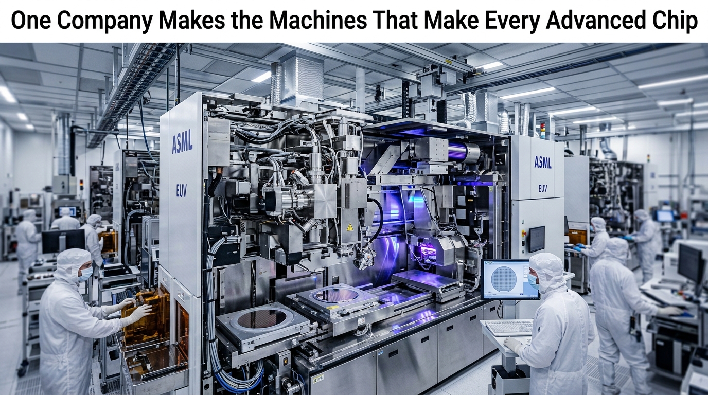
Molten tin is ejected as droplets, roughly 30 micrometres across, at a rate around 50,000 per second. Each droplet is struck in flight by a pulse from a high-power carbon dioxide laser. The pulse vaporises the tin into a plasma reaching temperatures of hundreds of thousands of degrees, and that plasma emits extreme ultraviolet light including the 13.5 nanometre wavelength required.
A collector mirror gathers the emitted light and directs it into the optical system. This must happen continuously, with each droplet hit accurately, for the machine to maintain output.
The engineering requirements this creates:
Droplet timing and tracking. Each droplet must be located and struck precisely, tens of thousands of times per second, indefinitely.
Laser power. The driving laser is among the most powerful industrial lasers in continuous operation, and its own reliability is a major concern.
Debris management. Vaporised tin deposits on surfaces. The collector mirror sits closest to the plasma and degrades over time, requiring periodic replacement — a significant maintenance cost.
Conversion efficiency. Only a small percentage of the laser energy becomes usable EUV light, which is why the input power must be so large.
Thermal management. Enormous power dissipation in a vacuum chamber containing precision optics that must remain dimensionally stable.
The result is a system consuming roughly a megawatt of electrical power to deliver a modest amount of light to the wafer. That inefficiency is a direct consequence of the physics rather than a design shortcoming.
Mirrors Instead of Lenses
Because transmissive optics are impossible, the entire imaging system is reflective, and the mirrors must be extraordinarily precise.
Surface figure tolerance is at the level of tens of picometres — a fraction of an atomic diameter. The frequently-used comparison is that if such a mirror were scaled to the size of a country, its largest surface deviation would be under a millimetre. This is not hyperbole; it is roughly the required specification.
Achieving it requires ion beam figuring, iterative measurement with interferometry at these tolerances, and multilayer coating deposited with atomic-scale thickness control across the whole surface. The number of organisations capable of producing these optics is very small — effectively one primary supplier for the highest-specification pieces.
The reflective architecture also imposes geometric constraints. Mirrors must be arranged so that incoming and outgoing light do not interfere with each other, which means off-axis illumination and a more complex optical layout than a lens system. Every mirror costs light, so the number is minimised, which constrains the achievable optical design.
This optical supply chain is a genuine single point of concentration. The machines depend on optics that essentially one company can make, which is a narrower constraint than the machine assembly itself.
The Mask Problem
Masks for EUV differ fundamentally from those used at longer wavelengths, and they introduce their own difficulties.
Conventional masks are transmissive — light passes through clear areas and is blocked by patterned ones. EUV masks must be reflective, since the light cannot pass through anything. They are multilayer mirrors with an absorbing pattern on top.
The consequences:
Defect-free multilayer stacks. A defect buried in the multilayer prints on every wafer, and repairing a buried defect is not possible. Producing defect-free blanks is a demanding manufacturing challenge in itself.
Pellicle difficulties. At longer wavelengths, a thin membrane protects the mask from particles. Any membrane absorbs EUV, so EUV pellicles must be extremely thin, which makes them fragile and reduces throughput. Operating without one means particles landing on the mask print defects.
Three-dimensional mask effects. The absorber layer has thickness comparable to the wavelength, and illumination is off-axis, so the pattern effectively shadows itself. This distorts the printed image in ways that must be corrected computationally in the mask design.
Inspection at these dimensions. Finding defects requires inspection tools operating at EUV wavelengths, which is a further specialised equipment category.
Mask cost for advanced nodes runs to very large sums per set, which is a significant component of why designing a leading-edge chip is so expensive and why the volume required to justify a design has risen.
Multipatterning and Why EUV Was Worth It
Understanding what EUV replaced clarifies its value.
With 193 nanometre immersion lithography, patterns finer than the tool could resolve were produced by splitting them across multiple exposures. Double patterning uses two exposures for one layer; quadruple patterning uses four, with additional etch and deposition steps between them.
The costs of this approach compound: each additional exposure adds process steps, so cycle time and cost rise. Overlay accuracy between exposures becomes critical, since misalignment between the sub-patterns produces defects. Design rules become restrictive, limiting what layouts are permissible. And yield falls as the number of steps increases.
By the time critical layers required quadruple patterning, the process complexity was substantial and the cost was rising faster than the density benefit.
EUV restored single-exposure patterning for those layers, which reduced the step count, improved cycle time, relaxed design rules, and improved yield. That is why the industry invested decades and enormous capital in making it work — not because shorter wavelength is inherently desirable, but because the alternative was becoming unaffordable.
Notably, EUV is now itself reaching the point where the most critical layers require multipatterning at 13.5 nanometres. Which is what motivates the next optical step.
High-NA and the Next Step
Resolution depends on wavelength divided by numerical aperture, the measure of how much light the optics collect. Since wavelength cannot easily go shorter, the remaining lever is numerical aperture.
High-NA EUV systems increase it from roughly 0.33 to 0.55, improving resolution meaningfully. The engineering consequences are substantial:
Anamorphic optics. The higher aperture requires different magnification in the two axes, which means the exposure field is halved in one dimension. A design larger than the field must be split across exposures and stitched.
Larger, more complex mirrors. More difficult and expensive to manufacture, at the same atomic-scale tolerances.
New mask requirements. Masks must accommodate the anamorphic imaging.
Reduced depth of focus. Higher aperture means less tolerance for wafer height variation, requiring tighter mechanical control.
Enormous cost. These machines are among the most expensive capital equipment items manufactured, and only the largest manufacturers can deploy them at scale.
The field size reduction is the consequential one for chip design. Large dies — which include the biggest accelerators and processors — will require stitching across exposures, and stitching introduces yield and design constraints. This interacts with the chiplet trend: designs partitioned into smaller pieces avoid the stitching problem entirely, which is another factor pushing toward chiplet architectures.
A Supply Chain With One Path
The concentration in this supply chain is worth stating plainly because it is unusual.
Exactly one company manufactures EUV lithography systems. Its machines contain optics from essentially one supplier, light sources dependent on specialised laser technology from a small number of sources, and tens of thousands of components from a supplier network built over decades.
Downstream, the number of manufacturers operating leading-edge fabs at scale is small, and geographically concentrated.
The implications are strategic rather than merely commercial. Every advanced processor, every high-end memory device, and every leading-edge accelerator depends on this chain. There is no second source at the equipment layer, and building one would take many years and enormous investment — the accumulated engineering knowledge is not readily replicated.
This concentration is why semiconductor equipment has become a subject of export policy and why supply chain resilience in this sector receives government attention. It is also why disruption at any point in the chain propagates broadly, and why capacity additions are measured in years rather than months.
For anyone reasoning about technology timelines, this is the constraint that bounds how quickly advanced chip capacity can grow. It is not primarily a matter of demand or investment — it is a matter of how many machines can be built.
Common Misconceptions
“Node names describe feature sizes.” They have been marketing designations for years rather than physical measurements. Actual dimensions differ substantially from the numbers.
“EUV is just a shorter wavelength.” It required abandoning transmissive optics, operating in vacuum, generating light by vaporising tin, and mirrors polished to atomic tolerances.
“Several companies make these machines.” One does. The optics come from essentially one supplier.
“EUV eliminated multipatterning.” For a period, at the most critical layers. The most advanced nodes are returning to multipatterning with EUV.
“More power solves the throughput problem.” Source power has improved enormously and remains a constraint, alongside optical losses that no amount of source power removes efficiently.
“Alternatives are nearly ready.” Electron beam and nanoimprint approaches exist for specific uses. Neither is a near-term replacement for high-volume patterning.
Conclusion
Advanced chip manufacturing depends on producing light at 13.5 nanometres, a wavelength that nothing transmits, by striking tin droplets with a high-power laser fifty thousand times per second, and reflecting the result off mirrors flat to a fraction of an atomic diameter, in a vacuum.
That system exists because the alternative — splitting patterns across four or more exposures with 193 nanometre light — was becoming economically unsustainable. EUV restored single-exposure patterning for critical layers, which reduced process steps and improved yield enough to justify decades of development.
The next step raises numerical aperture rather than shortening wavelength further, which halves the exposure field and pushes large designs toward being split into pieces — reinforcing the move to chiplet architectures for reasons unrelated to yield.
And the whole chain narrows to one equipment supplier depending on essentially one optics supplier. That concentration is the industry’s tightest constraint, it cannot be resolved quickly, and it is why advanced chip capacity grows on timelines measured in years.
Frequently Asked Questions
Why can lenses not be used at EUV wavelengths? Essentially all materials absorb rather than transmit 13.5 nanometre light. The optical system must be entirely reflective, using multilayer mirrors that themselves reflect only around 70 percent.
Why vaporise tin specifically? Tin plasma emits efficiently at 13.5 nanometres, which is the wavelength the multilayer mirror coatings are designed to reflect. The wavelength and the material choice are coupled.
Do process node names mean anything physical? Not directly. They have been marketing designations for years. Actual transistor dimensions and density must be compared using published density figures rather than node names.
Why is only one company able to build these machines? Decades of accumulated engineering, a supplier network built specifically for it, and the optics requirement that essentially one company can meet. Replicating it would take many years and enormous investment.
What does High-NA change for chip designers? The exposure field halves in one dimension, so large dies must be stitched across exposures. This adds constraints and is another reason to partition designs into chiplets.
Are there alternatives to EUV? Electron beam lithography is used for mask making and is far too slow for wafer production. Nanoimprint has specific applications. Neither replaces EUV for high-volume advanced patterning in the near term.
Why does EUV consume so much power? Low conversion efficiency from laser energy to usable EUV, compounded by roughly 30 percent loss at each of about ten mirrors. Most generated light never reaches the wafer, so the source must vastly overproduce.


